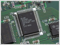
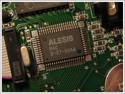
Alesis M4 and M4C (M4 revision C) DSP ASIC
Designed and formerly produced by Alesis Semiconductor
and then - Wavefront Semiconductor. The M4 and M4C is
used in
MidiVerb4, MicroVerb4, NanoVerb and probably also in some compact mixing
consoles with effects.
Two main classic Alesis chip designers moved on to fund their own company: Spin Semiconductor.
While that chip is old (finished in 1993) and does not represent the extreme signal
processing monsters league, it still has some interesting aspects -
mostly as a good example of a system design simplification and
integration. There's almost no information about it (or even insides of
MidiVerb4) on the web, so I decided to put here some of the notes
about it, that might also be useful for repairs. For DSP zealots I
will also dump here some übersecret info on it's operation and
algorithms.
M4 (p/n 2-27-0031) is used in MidiVerb 4 and early MicroVerb4 (rev.A and probably B as well)
M4C (p/n 2-27-0044) is used in MicroVerb 4 (rev.C and later), NanoVerb and seems also on later MidiVerb 4 units
As a somewhat oldschool design, chip is entirely 5V.
For every sample it executes 64 x 32bit instructions, each
consisting
of a several wcs microcode parts and a memory offset (which can be
further offset by lfo). For each instruction cycle it needs eight
clocks to work all the things including the multiplier - the design so
optimized and clever that I'm very tempted to recreate one on a CPLD!
I've made disassembler for it and other stuff that I will at some point
make a separate page about.
 | Besides DSP stuff, M4 also has:
|
 | Besides DSP stuff, M4C also has:
|
For the M4C, memory transfer rate is about one third to one sixth in
comparison to
other manufacturer system designs of that day. However, it was a cost
effective solution, to use only one DRAM chip and access memory by
nibbles (thus making things four times slower). On newer board versions
(after 2000), when old DRAM chips got phased out and Alesis had to
switch to contemporary parts, things got even less pretty, as the M4C
chip there actually uses only one fourth of the available bandwidth and
amount of memory of the attached 16bit DRAM chip. The remaining 3/4 of
the
memory and speed is unused and therefore sadly wasted.
Nonetheless, chip is very capable and there are some
wonderful sounding algos working on it. Thank You Keith, Frank and David for the amazing
programs! :)
Any of it's effects DSP programs (even the magnificent reverb with
swirl and filters, as well as combinations of chorus>delay>room) fit in
just 64 instructions. One of the simplest things, the mono delay (that has two filters in it), fits
in just 18 instructions. Auto Panner (that also has two filters in it) is even smaller - only 17 instructions.
Instructions are 32bit wide, and, by the way, original assembler uses $00000303 as a NOP - a
heartwarming "♥ ♥" when viewed in ASCII!
Page currently under development. Someday I hope to
dump there my papers on system memory map, access timing, wcs microcode, bootup and
realtime effects control.
Alesis M4 chip pinout
| pin number | short name | description |
| VCC | Supply 5V | |
| GND | ||
| 4,3,2,1,64,63,62,61 | D0..D7 | CPU address/data bus |
| 9 |
ALE |
Input; CPU address latch enable |
| 17,16,15,14,13,12,11,10 |
A0..A7 |
Outputs of the ALE latch, for the CPU ROM&RAM |
| 6, 5 |
A15, A12 |
Inputs of two CPU address lines for memory mapped stuff decoder |
| 19 |
CPUCLK |
Output; clock for CPU (12MHz) |
| 7 |
/RD |
Input |
| 8 |
/WR |
Input |
| 56 |
/RESOUT |
Output; reset to CPU |
| 53 |
/SRAMCE |
Output; Chip enable for controller's SRAM chip |
| 55 |
RES |
Input; reset, active high, probably has a high treshold level (I haven't measured) |
| 21 |
LRCK |
Output; Audio ADC/DAC usual stuff |
| 23 |
SDI |
Input; Audio ADC/DAC usual stuff - bit input from ADC |
| 22 |
SDO |
Output; Audio ADC/DAC usual stuff - bit output to DAC |
| 20 |
SCK |
Output; Audio ADC/DAC usual stuff - bit clock (3.072MHz) |
| 18 |
NANDTREEOUT |
Test pin |
| 42,41,40,39,38,37,36,35, 34,33,32,31,30,29,28,25,24 |
DSPSRAMA0..DSPSRAMA16 |
Address bus outputs to DSP SRAM |
| 43 |
/DSPSRAMOE |
|
| 44 |
/DSPSRAMWR |
Output to DSP SRAM; Write enable (active low) |
| 52,51,50,49,48,47,46,45 |
DSPSRAMD0..DSPSRAMD7 |
DSP SRAM data bus |
| 54 |
LCDEN |
Output; LCD chip select, active high |
| 59, 60 |
XIN, XOUT |
Quartz loop, 24MHz, no additional external components required |
Alesis M4C (M4 revision C) chip pinout
| pin number | short name | description |
| 1, 33, 52 | VCC | Supply 5V |
| 19, 51, 64 | GND | |
| 2,3,4,5,6,7,8,9 | D0..D7 | CPU data bus |
| 10 |
ALE |
Input; CPU address latch enable |
| 11,12,13,14,15,16,17,18 |
A0..A7 |
Outputs of the ALE latch, for the CPU ROM&RAM |
| 20, 21 |
A15, A12 |
Inputs of two CPU address lines |
| 22 |
CPUCLK |
Output; clock for CPU (12MHz) |
| 23 |
/RD |
Input |
| 24 |
/WR |
Input |
| 25 |
/RESOUT |
Output; reset to CPU |
| 26 |
/SRAMCE |
Output; Chip enable for SRAM chip |
| 27 |
RES |
Input; reset, active high, probably has a high treshold level (I haven't measured) |
| 28 |
LRCK |
Output; Audio ADC/DAC usual stuff |
| 29 |
SDI |
Input; Audio ADC/DAC usual stuff - bit input from ADC |
| 30 |
SDO |
Output; Audio ADC/DAC usual stuff - bit output to DAC |
| 31 |
SCK |
Output; Audio ADC/DAC usual stuff - bit clock (3.072MHz) |
| 32 |
NANDTREEOUT |
Test pin |
| 42,41,40,39,38,37,36,35,34 |
DRAMA0..DRAMA8 |
Address bus outputs to DRAM |
| 43 |
/CAS |
Output to DRAM; Column address strobe |
| 44 |
/RAS |
Output to DRAM; Row address strobe |
| 45 |
/DRAMWE |
Output to DRAM; Write enable (active low) |
| 50,49,47,46 |
DRAMD0..DRAMD3 |
DRAM data bus |
| 48 |
TEST |
Normally connected to ground |
| 53 |
LCDE |
Output; LCD chip select, active high |
| 54 |
VCOEN |
Input; Enables the VCO stuff when high. Connect to gnd when using with OSC |
| 55, 56 |
XIN, XOUT |
Quartz loop, 24MHz, no additional external components required |
| 57 |
VA |
Supply 5V |
| 58 |
VCOIN |
Input; VCO steering |
| 59 |
ADCREF |
Analog input; ADC ref level, normally supplied with 3.75V from the upper side of pots |
| 60,61 |
ADCIN0, ADCIN1 |
Analog input; ADC input to be connected to a fader or pot. Input range: GND..ADCREF |
| 62 |
RIOUT |
This pin is connected to 10uF capacitor, that is in series to +5V |
| 63 |
C2 |
This pin is connected to a 2200pF capacitor, that is in series to GND |